- 您现在的位置:买卖IC网 > Sheet目录1905 > ATMEGA644P-B15MZ (Atmel)IC MCU 8BIT 64KB FLASH 32VQFN
14
7674F–AVR–09/09
ATmega164P/324P/644P
5.5.1
SPH and SPL – Stack Pointer High and Stack pointer Low
5.6
Instruction Execution Timing
This section describes the general access timing concepts for instruction execution. The AVR
CPU is driven by the CPU clock clk
CPU, directly generated from the selected clock source for the
chip. No internal clock division is used.
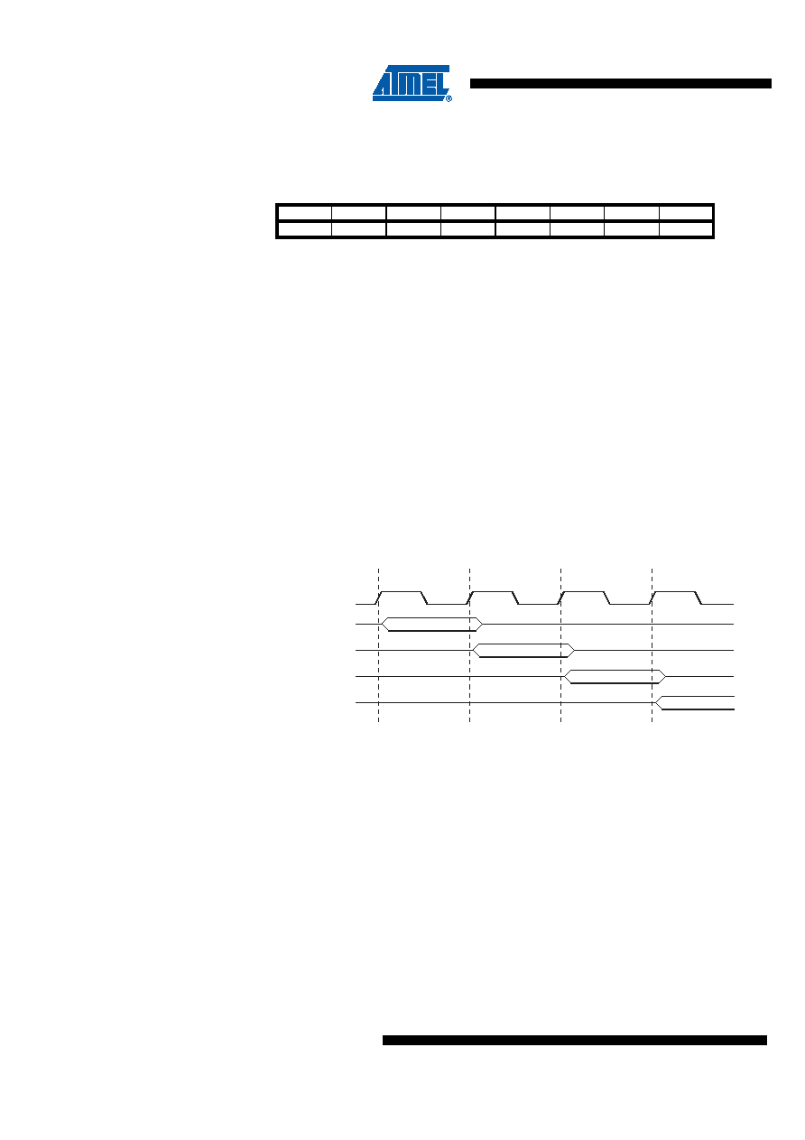
Figure 5-4 on page 14 shows the parallel instruction fetches and instruction executions enabled
by the Harvard architecture and the fast-access Register File concept. This is the basic pipelin-
ing concept to obtain up to 1 MIPS per MHz with the corresponding unique results for functions
per cost, functions per clocks, and functions per power-unit.
Figure 5-4.
The Parallel Instruction Fetches and Instruction Executions
Figure 5-5 shows the internal timing concept for the Register File. In a single clock cycle an ALU
operation using two register operands is executed, and the result is stored back to the destina-
tion register.
Bit
151413121110
9
8
–
SP12
SP11
SP10
SP9
SP8
SPH
SP7
SP6
SP5
SP4
SP3
SP2
SP1
SP0
SPL
765
432
10
Read/Write
R
R/W
Initial Value
0
1
0
111
11
clk
1st Instruction Fetch
1st Instruction Execute
2nd Instruction Fetch
2nd Instruction Execute
3rd Instruction Fetch
3rd Instruction Execute
4th Instruction Fetch
T1
T2
T3
T4
CPU
发布紧急采购,3分钟左右您将得到回复。
相关PDF资料
ATMEGA644V-10PU
IC AVR MCU FLASH 64K 40DIP
ATMEGA645V-8MI
IC AVR MCU FLASH 64K 1.8V 64QFN
ATMEGA649-16MI
IC AVR MCU FLASH 64K 5V 64QFN
ATMEGA649V-8MI
IC AVR MCU FLASH 64K 1.8V 64QFN
ATMEGA8515L-8JUR
MCU AVR 8KB FLASH 8MHZ 44PLCC
ATMEGA8515L-8PJ
IC MCU AVR 8K 5V 8MHZ 40-DIP
ATMEGA8535-16JUR
MCU AVR 8K FLASH 16MHZ 44PLCC
ATMEGA8535L-8PJ
IC MCU AVR 8K 5V 8MHZ 40-DIP
相关代理商/技术参数
ATMEGA644PR212-AU
功能描述:8位微控制器 -MCU ATmega 644PV-10AU AT86RF212-ZU RoHS:否 制造商:Silicon Labs 核心:8051 处理器系列:C8051F39x 数据总线宽度:8 bit 最大时钟频率:50 MHz 程序存储器大小:16 KB 数据 RAM 大小:1 KB 片上 ADC:Yes 工作电源电压:1.8 V to 3.6 V 工作温度范围:- 40 C to + 105 C 封装 / 箱体:QFN-20 安装风格:SMD/SMT
ATMEGA644PR212-MU
功能描述:8位微控制器 -MCU ATmega 644PV-10MU AT86RF212-ZU RoHS:否 制造商:Silicon Labs 核心:8051 处理器系列:C8051F39x 数据总线宽度:8 bit 最大时钟频率:50 MHz 程序存储器大小:16 KB 数据 RAM 大小:1 KB 片上 ADC:Yes 工作电源电压:1.8 V to 3.6 V 工作温度范围:- 40 C to + 105 C 封装 / 箱体:QFN-20 安装风格:SMD/SMT
ATMEGA644PR231-AU
功能描述:8位微控制器 -MCU ATmega 644PV-10AU AT86RF231-ZU RoHS:否 制造商:Silicon Labs 核心:8051 处理器系列:C8051F39x 数据总线宽度:8 bit 最大时钟频率:50 MHz 程序存储器大小:16 KB 数据 RAM 大小:1 KB 片上 ADC:Yes 工作电源电压:1.8 V to 3.6 V 工作温度范围:- 40 C to + 105 C 封装 / 箱体:QFN-20 安装风格:SMD/SMT
ATMEGA644PR231-MU
功能描述:8位微控制器 -MCU ATmega 644PV-10MU AT86RF231-ZU RoHS:否 制造商:Silicon Labs 核心:8051 处理器系列:C8051F39x 数据总线宽度:8 bit 最大时钟频率:50 MHz 程序存储器大小:16 KB 数据 RAM 大小:1 KB 片上 ADC:Yes 工作电源电压:1.8 V to 3.6 V 工作温度范围:- 40 C to + 105 C 封装 / 箱体:QFN-20 安装风格:SMD/SMT
ATMEGA644PV-10AQ
功能描述:8位微控制器 -MCU AVR 64KB, 2KB EE 20MHz 4KB SRAM, 1.8V RoHS:否 制造商:Silicon Labs 核心:8051 处理器系列:C8051F39x 数据总线宽度:8 bit 最大时钟频率:50 MHz 程序存储器大小:16 KB 数据 RAM 大小:1 KB 片上 ADC:Yes 工作电源电压:1.8 V to 3.6 V 工作温度范围:- 40 C to + 105 C 封装 / 箱体:QFN-20 安装风格:SMD/SMT
ATMEGA644PV-10AQR
功能描述:8位微控制器 -MCU AVR 64KB FLSH 2KB EE 4KB SRAM-20MHz, 5V RoHS:否 制造商:Silicon Labs 核心:8051 处理器系列:C8051F39x 数据总线宽度:8 bit 最大时钟频率:50 MHz 程序存储器大小:16 KB 数据 RAM 大小:1 KB 片上 ADC:Yes 工作电源电压:1.8 V to 3.6 V 工作温度范围:- 40 C to + 105 C 封装 / 箱体:QFN-20 安装风格:SMD/SMT
ATMEGA644PV-10AU
功能描述:8位微控制器 -MCU AVR 64K FLASH 2K EE 4K SRAM ADC-10MHZ RoHS:否 制造商:Silicon Labs 核心:8051 处理器系列:C8051F39x 数据总线宽度:8 bit 最大时钟频率:50 MHz 程序存储器大小:16 KB 数据 RAM 大小:1 KB 片上 ADC:Yes 工作电源电压:1.8 V to 3.6 V 工作温度范围:- 40 C to + 105 C 封装 / 箱体:QFN-20 安装风格:SMD/SMT
ATMEGA644PV-10AUR
功能描述:8位微控制器 -MCU AVR 64KB FLSH 2KB EE 4KB SRAM-10MHz, 1.8V RoHS:否 制造商:Silicon Labs 核心:8051 处理器系列:C8051F39x 数据总线宽度:8 bit 最大时钟频率:50 MHz 程序存储器大小:16 KB 数据 RAM 大小:1 KB 片上 ADC:Yes 工作电源电压:1.8 V to 3.6 V 工作温度范围:- 40 C to + 105 C 封装 / 箱体:QFN-20 安装风格:SMD/SMT